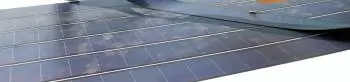
Thin-film solar cells are the second generation of solar cells. These cells are built by depositing one or more thin layers or thin film (TF) of photovoltaic material on a substrate, such as glass, plastic, or metal.
The thickness of the film varies from a few nanometers (nm) to tens of micrometers (µm). The film is much thinner than the first-generation conventional crystalline silicon (c-Si) solar cell, which uses wafers up to 200 µm thick.
It allows thin-film cells to be flexible and lighter in weight.
Much research is currently being invested in increasing the efficiency of these technologies as they promise to achieve the goal of low-cost, high-efficiency production.
Where are thin-film solar cells used?
It is used in constructing integrated photovoltaic power systems and as a semi-transparent photovoltaic glazing material that can be laminated into windows.
Some commercial uses use rigid thin-film solar panels (sandwiched between two glass panes) in some of the world's largest photovoltaic power plants.
These solar cells are also a good option for use in spacecraft due to their low weight.
Types of thin-film photovoltaic cells
Many photovoltaic materials are manufactured using different deposition methods on various substrates. Therefore, thin-film solar cells are generally classified according to the photovoltaic material used. According to these criteria, the following types of thin-film photovoltaic cells are found.
-
Amorphous silicon (a-Si) and other thin-film silicones (TF-Si)
-
Cadmium telluride (CdTe)
-
Gallium indium copper selenide (CIS or CIGS)
-
Color-sensitive solar cells (DSC) and other organic solar cells.
-
Gallium arsenide (GaAs)
Cadmium telluride (CdTe)
Cadmium telluride is the most advanced thin-film technology. Approximately half of the world's production of photovoltaic panels and more than half of the market for thin films are in the hands of this technology.
In vitro cell efficiency has increased in recent years and is in line with CIGS thin-film and close to the efficiency of multi-crystalline silicon.
While environmental concerns about cadmium toxicity can be fully remedied by recycling cadmium at the end of its period. The use of scarce materials can also be a problem for the economic viability of this type of cell.
Copper indium gallium selenide (CIGS)
Selenide gallium or CIGS photovoltaic cell uses an adsorbent of selenium gallium indium and copper, the other types of free gallium being abbreviated CIS.
This technology is one of the three main streams of thin-film cells. The other two are cadmium telluride and amorphous silicon, which has a laboratory efficiency of 5% and a market share of 5%.
Amorphous silicon thin-film solar cell
Amorphous silicon solar cells are multiple forms of non-crystalline silicon and have been the most advanced thin-film technology to date. Silicon-based products are less problematic than CIS and CdTe products.
These cells can be passivated by hydrogen during the manufacturing process. It bonds to dangling bonds and can significantly reduce dangling bond density. In addition, hydrogenated amorphous silicon (a-Si: H) has a sufficiently low amount of defects to be used in PV solar panels.
Furthermore, there is no objection to the use of standard silicon as a result of political resistance to the use of non-green materials in solar energy production.
Silicon modules are divided into three categories:
-
Amorphous silicon photovoltaic cells
-
Multicrystalline tandem photovoltaic cells
-
Multicrystalline silicon thin film on glass
The conversion efficiency of thin-film modules
Thin film technology has always been cheaper but less efficient than conventional c-Si technology. However, it has improved significantly over the years.
Laboratory cell efficiency for CdTe and CIGS now exceeds 21 percent, outperforming multi-crystalline silicon, the dominant material currently used in most solar PV systems.
Accelerated life tests of thin-film junction solar cells under laboratory conditions measured somewhat faster degradation than conventional PV, while a lifespan of 20 years or more is generally expected.
Optimization of thin-film solar cells
Multiple techniques have been used to increase the amount of light entering the cell and reduce the amount that escapes without absorption.
Minimization of the upper contact coverage of the cell surface
The most obvious technique is to minimize the upper contact coverage of the cell surface, reducing the area that prevents light from reaching the cell.
The weakly absorbed long wavelength light can be obliquely coupled to the silicon and passes through the film several times to improve absorption.
Minimization of the number of photons reflected away
There are many methods to increase absorption by reducing the number of incident photons reflected away from the cell surface. An additional anti-reflective coating can cause destructive interference within the cell by modulating the refractive index of the surface coating. It eliminates the reflective wave, causing all incident light to enter the solar cell.
Surface texturing
Surface texturing is another option to increase absorption, but it increases costs. By applying a texture to the surface of the active material, the reflected light can be refracted to strike the surface again, thereby reducing the reflectance.
For example, the texture of black silicon by reactive ionic etching (RIE) is an effective and economical approach to increase the absorption of thin-film silicon solar cells. In addition, a textured rear reflector can prevent light from escaping from the back of the cell.
In addition to the surface texture, the plasmonic light capture scheme attracted a lot of attention to help improve the photocurrent in thin-film solar cells. This method uses the collective oscillation of excited free electrons in nanoparticles of noble metals, which are influenced by the shape of the particles, the size, and the dielectric properties of the surrounding medium.
Solar cell material optimization
In addition to minimizing the reflective loss, the solar cell material can be optimized to have a greater chance of absorbing a photon that reaches it. As a result, thermal processing techniques can significantly improve the crystal quality of silicon cells and, therefore, increase efficiency.
The thin-film cell layer can also create a multiple junction solar cell. The band interval of each layer can be designed to absorb a different range of wavelengths better so that together they can absorb a greater spectrum of light.
Geometric design
Further progress in geometric considerations can exploit the nanomaterial's dimensionality. Large parallel nanowire matrices allow long absorption lengths along the length of the cable while maintaining short diffusion lengths of minor carriers along the radial direction.
Adding nanoparticles between the nanowires allows conduction. The natural geometry of these matrices forms a textured surface that catches more light.