Monocrystalline silicon is the base material for silicon chips used in virtually all electronic equipment today. In the field of solar energy, monocrystalline silicon is also used to make photovoltaic cells due to its ability to absorb radiation.
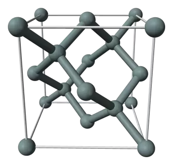
Monocrystalline silicon consists of silicon in which the crystal lattice of the entire solid is continuous. This crystalline structure does not break at its edges and is free of any grain boundaries.
Monocrystalline silicon can be prepared as:
-
An intrinsic semiconductor that is composed only of very pure silicon
-
It can also be doped by adding other elements such as boron or phosphorus.
Monocrystalline silicon in solar panels
Monocrystalline silicon is used to manufacture high-performance photovoltaic panels.
The quality requirements for monocrystalline solar panels are not very demanding. In this type of boards the demands on structural imperfections are less high compared to microelectronics applications. For this reason, lower quality silicon is used.
Despite this, the monocrystalline silicon solar PV industry has improved considerably.
Manufacture of monocrystalline silicon photovoltaic panels
In addition to the low production rate, there are also concerns about wasted material in the manufacturing process.
Creating space-saving solar panels requires cutting circular wafers into octagonal cells that can be packed together. Circular wafers are a product of cylindrical ingots formed through the Czochralski process.
The leftover material is not used to create photovoltaic cells and is discarded or recycled back into ingot production for fusion.
Monocrystalline silicon cells can absorb most photons within 20 μm of the incident surface. However, limitations in the ingot sawing process mean that the commercial wafer thickness is generally around 200 μm.
Efficiency in photovoltaic panels
This type of silicon has a recorded single cell laboratory efficiency of 26.7%. This means it has the highest confirmed conversion efficiency of all commercial PV technologies.
The high efficiency is attributed to:
-
A lack of recombination sites in the single crystal
-
Better photon absorption due to its black color, compared to the characteristic blue tone of poly-silicon.
Monocrystalline cells are more expensive than polycrystalline cells. For this reason, mono-Si cells are useful for applications where the main considerations are weight or available area limitations.
This type of panels are used, for example, in spacecraft or satellites powered by solar energy. In these cases, furthermore, efficiency can be further improved by combining other technologies, such as multilayer solar cells.
Manufacturing and production
Monocrystalline silicon is typically created by one of several methods that involve melting high-purity semiconductor-grade silicon and using a seed to initiate the formation of a continuous single crystal.
This process is typically performed in an inert atmosphere, such as argon, and in an inert crucible, such as quartz. In this way, impurities that would affect the uniformity of the glass are avoided.
Compared to polycrystalline ingot molding, monocrystalline silicon production is very slow and expensive. However, the demand for monocrystalline silicon continues to increase due to superior electronic properties.
Czochralski Process
The most common production method for monocrystalline silicon is the Czochralski process. This process involves immersing a seed crystal mounted on rods precisely into molten silicon.
The bar is then slowly pulled up and rotated simultaneously. This allows the stretched material to solidify into a monocrystalline cylindrical ingot up to 2 meters long and weighing several hundred kilograms.
Magnetic fields can also be applied to control and suppress turbulent flow, further improving crystallization uniformity.
Other manufacturing methods
Other methods are:
The growth of the floating zone, which passes a polycrystalline silicon rod through a radio frequency heating coil. This coil creates a localized molten zone, from which a seed crystal ingot grows.
Bridgman techniques move the crucible through a temperature gradient to cool it from the end of the container containing the seed. The solidified ingots are cut into thin sheets for further processing.